
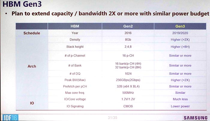
Despite first- and second-generation High Bandwidth Memory having made few appearances in shipping products, Samsung and Hynix are already working on a followup: HBM3. Teased at the Hot Chips symposium in Cupertino, Calfornia, HBM3 will offer improved density, bandwidth, and power efficiency. Perhaps most importantly though, given the high cost of HBM1 and HBM2, HBM3 will be cheaper to produce.
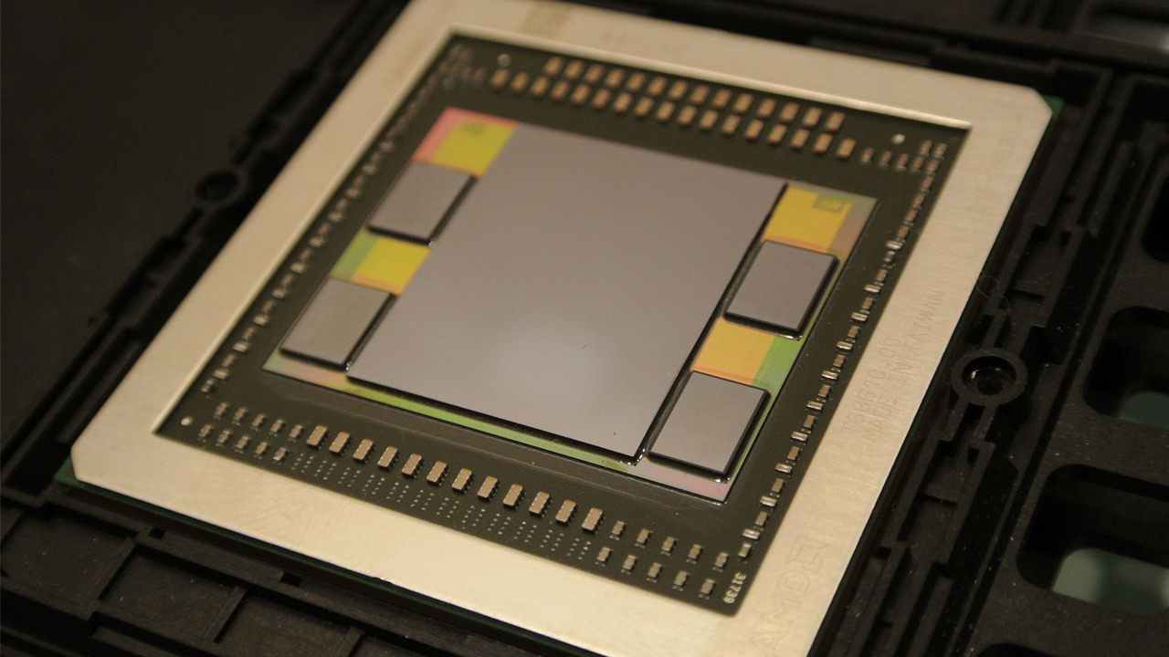
With conventional memory setups, RAM chips are placed next to each other on a circuit board, usually as close as possible to the logic device (CPU or GPU) that needs access to the RAM. HBM, however, stacks a bunch of RAM dies (dice?) on top of each other, connecting them directly with through-silicon vias (TSVs). These stacks of RAM are then placed on the logic chip package, which reduces the surface area of the device (AMD's Fury Nano is a prime example), and potentially provides a massive boost in bandwidth.
The tradeoff, though, as with most fancy packaging techniques, has been price and capacity. HBM1, as used in AMD's Fury graphics cards, was limited to 4GB stacks. HBM2, as used in Nvidia's workstation-only P100 graphics card, features higher density stacks up up to 16GB, but is prohibitively expensive for consumer cards.
HBM3 will double density of the individual memory dies from 8Gb to 16Gb (~2GB), and will allow for more than eight dies to be stacked together in a single chip. Graphics cards with up to 64GB of memory are possible.
HBM3 will feature a lower core voltage than the 1.2V of HBM2, as well as more than two times the peak bandwidth: HBM2 offers 256GB/s of bandwidth per layer of DRAM, while HBM3 doubles that to 512GB/s. The total amount of memory bandwidth available could well be terabytes per second.
Both Hynix and Samsung are working on HBM3 (Samsung is calling its version "Extreme HBM"), although neither has committed to a firm release date. AMD's current GPU roadmap points to its Navi architecture—the follow up to Vega, which itself follows Polaris—using "NextGen memory," and is due for release in 2018.
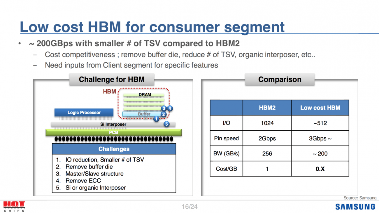
In addition to HMB3, Samsung unveiled two other memory technologies at Hot Chips: GDDR6 and "Low Cost" HBM. GDDR6 is the successor to GDDR5X—as used in Nvidia's GTX 1080—and is scheduled for release in 2018. GDDR6 promises per-pin bandwidth of over 14Gbps, up from 10Gbps, as well as greater power efficiency. Further details are promised at a later date.
Meanwhile, Samsung has been working on making HBM cheaper by removing the buffer die, and reducing the number of TSVs and interposers. While these changes will have an impact on the overall bandwidth, Samsung has increased the individual pin speed from 2Gbps to 3Gbps, offsetting the reductions somewhat. HBM2 offers around 256GB/s bandwidth, while low cost HBM will feature approximately 200GB/s of bandwidth. Pricing is expected to be far less than that of HBM2, with Samsung targeting mass market products.
reader comments
47