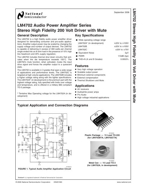
LM4702 Audio Power Amplifier Series Stereo High Fidelity 200 Volt ...
LM4702 Audio Power Amplifier Series Stereo High Fidelity 200 Volt ...
LM4702 Audio Power Amplifier Series Stereo High Fidelity 200 Volt ...

You also want an ePaper? Increase the reach of your titles
YUMPU automatically turns print PDFs into web optimized ePapers that Google loves.
<strong>LM4702</strong> <strong>Audio</strong> <strong>Power</strong> <strong>Amplifier</strong> <strong>Series</strong><br />
<strong>Stereo</strong> <strong>High</strong> <strong>Fidelity</strong> <strong>200</strong> <strong>Volt</strong> Driver with Mute<br />
General Description<br />
The <strong>LM4702</strong> is a high fidelity audio power amplifier driver<br />
designed for demanding consumer and pro-audio applications.<br />
<strong>Amplifier</strong> output power may be scaled by changing the<br />
supply voltage and number of output devices. The <strong>LM4702</strong><br />
is capable of delivering in excess of 300 watts per channel<br />
single ended into an 8 ohm load in the presence of 10% high<br />
line headroom and 20% supply regulation.<br />
The <strong>LM4702</strong> includes thermal shut down circuitry that activates<br />
when the die temperature exceeds 150˚C. The<br />
<strong>LM4702</strong>’s mute function, when activated, mutes the input<br />
drive signal and forces the amplifier output to a quiescent<br />
state.<br />
The <strong>LM4702</strong> is available in 3 grades that span a wide range<br />
of applications and performance levels. The <strong>LM4702</strong>C is<br />
targeted at high volume applications. The <strong>LM4702</strong>B includes<br />
a higher voltage rating along with the tighter specifications.<br />
The <strong>LM4702</strong>A* (in development) is the premium part with the<br />
highest voltage rating, fully specified with limits over voltage<br />
and temperature, and is offered in a military 883 compliant<br />
TO-3 package.<br />
* Tentative Max Operating voltage for the <strong>LM4702</strong>A (in development)<br />
Typical Application and Connection Diagrams<br />
20158319<br />
FIGURE 1. Typical <strong>Audio</strong> <strong>Amplifier</strong> Application Circuit<br />
Overture ® is a registered trademark of National Semiconductor Corporation.<br />
Key Specifications<br />
j Wide operating voltage range<br />
<strong>LM4702</strong>A* (in development) ±20V to ±100V<br />
<strong>LM4702</strong>B ±20V to ±100V<br />
<strong>LM4702</strong>C ±20V to ±75V<br />
j Equivalent Noise 3µV<br />
j PSRR 110dB (typ)<br />
j THD+N (A and B Grades) 0.0003%<br />
Features<br />
n Very high voltage operation<br />
n Scalable output power<br />
n Minimum external components<br />
n External compensation<br />
n Thermal Shutdown and Mute<br />
Applications<br />
n AV receivers<br />
n <strong>Audio</strong>phile power amps<br />
n Pro <strong>Audio</strong><br />
n <strong>High</strong> voltage industrial applications<br />
20158302<br />
Plastic Package — 15 Lead TO-220<br />
(for <strong>LM4702</strong>BTA, <strong>LM4702</strong>CTA)<br />
20158320<br />
Metal Can — 15 Lead TO-3<br />
(for <strong>LM4702</strong>A, in development)<br />
September <strong>200</strong>6<br />
© <strong>200</strong>6 National Semiconductor Corporation DS201583 www.national.com<br />
<strong>LM4702</strong> <strong>Stereo</strong> <strong>High</strong> <strong>Fidelity</strong> <strong>200</strong> <strong>Volt</strong> Driver with Mute
<strong>LM4702</strong><br />
Typical Application and Connection Diagrams (Continued)<br />
FIGURE 1. Typical <strong>Audio</strong> <strong>Amplifier</strong> Application Circuit<br />
www.national.com 2<br />
20158319
Connection Diagram<br />
Plastic Package (For B and C) (Note 13)<br />
Top View<br />
Order Number <strong>LM4702</strong>BTA, <strong>LM4702</strong>CTA<br />
See NS Package Number TA15A<br />
3<br />
20158301<br />
www.national.com<br />
<strong>LM4702</strong>
<strong>LM4702</strong><br />
Absolute Maximum Ratings (Notes 1,<br />
2)<br />
If Military/Aerospace specified devices are required,<br />
please contact the National Semiconductor Sales Office/<br />
Distributors for availability and specifications.<br />
Supply <strong>Volt</strong>age |V + |+|V- |<br />
C Part <strong>200</strong>V<br />
A, B Parts <strong>200</strong>V<br />
Differential Input <strong>Volt</strong>age +/-6V<br />
Common Mode Input Range 0.4 Vee to 0.4 Vcc<br />
<strong>Power</strong> Dissipation (Note 3) 4W<br />
ESD Susceptibility (Note 4) 1.5kV<br />
ESD Susceptibility (Note 5) <strong>200</strong>V<br />
Junction Temperature (TJMAX) (Note 9)<br />
Soldering Information<br />
150˚C<br />
T Package (10 seconds) 260˚C<br />
Storage Temperature -40˚C to +150˚C<br />
Thermal Resistance<br />
θJA 30˚C/W<br />
1˚C/W<br />
θ JC<br />
Operating Ratings (Notes 1, 2)<br />
Temperature Range<br />
TMIN ≤ TA ≤ TMAX Supply <strong>Volt</strong>age |V<br />
−20˚C ≤ TA ≤ +75˚C<br />
+ |+|V- |<br />
<strong>LM4702</strong>A (in development) +/-20V ≤ VTOTAL ≤ +/-100V<br />
<strong>LM4702</strong>B +/-20V ≤ VTOTAL ≤ +/-100V<br />
<strong>LM4702</strong>C +/-20V ≤ VTOTAL ≤ +/-75V<br />
Electrical Characteristics (<strong>LM4702</strong>C) Vcc = +75V, Vee = –75V (Notes 1, 2)<br />
The following specifications apply for IMUTE = 1.5mA, Figure 1, unless otherwise specified. Limits apply for TA = 25˚C.<br />
Symbol Parameter Conditions <strong>LM4702</strong> Units<br />
Typical Limit (Limits)<br />
(Note 6) (Notes 7, 8)<br />
Total Quiescent <strong>Power</strong> Supply<br />
Current<br />
VCM = 0V, VO = 0V, IO = 0A 25 30 mA (max)<br />
I CC<br />
THD+N<br />
Total Harmonic Distortion +<br />
Noise<br />
No load, A V = 30dB<br />
V OUT = 14V RMS @ 1kHz<br />
0.005 %<br />
RS Input Bias Resistor 50 100 kΩ (max)<br />
Av Closed Loop <strong>Volt</strong>age Gain 26 dB (min)<br />
Av open Open Loop Gain Vin = 1mVrms, f = 1KHz, C = 30pF 93 dB<br />
Vom Output <strong>Volt</strong>age Swing THD = 0.05%, Freq = 20Hz to 20KHz 51 Vrms (min)<br />
Vnoise Output Noise<br />
Rs = 10kΩ, LPF = 30kHz, Av = 30dB<br />
A-weighted<br />
I OUT Output Current Current from Source to Sink Pins 5.5<br />
I mute Current into Mute Pin To put part in “play” mode 1.5<br />
150 300 µV (max)<br />
90 µV<br />
3<br />
10<br />
1<br />
2<br />
mA(min)<br />
mA (max)<br />
mA(min)<br />
mA (max)<br />
X TALK Channel Separation (Note 11) f = 1kHz @ Av = 30dB 85 dB<br />
SR Slew Rate<br />
VIN = 1.2VP-P, f = 10kHz square Wave,<br />
Outputs shorted<br />
15 V/µs<br />
VOS Input Offset <strong>Volt</strong>age VCM = 0V, IO = 0mA 10 35 mV (max)<br />
IB Input Bias Current VCM = 0V, IO = 0mA 500 nA<br />
PSRR <strong>Power</strong> Supply Rejection Ratio<br />
Rs = 1k, f = 100Hz,<br />
Vripple = 1Vrms, Input Referred<br />
110 95 dB (min)<br />
Electrical Characteristics (<strong>LM4702</strong>C) Vcc = +50V, Vee = –50V (Notes 1, 2)<br />
The following specifications apply for IMUTE = 1.5mA, Figure 1, unless otherwise specified. Limits apply for TA = 25˚C.<br />
Symbol Parameter Conditions <strong>LM4702</strong> Units<br />
Typical Limit (Limits)<br />
(Note 6) (Notes 7, 8)<br />
Total Quiescent <strong>Power</strong> Supply<br />
Current<br />
VCM = 0V, VO = 0V, IO =0A<br />
22 30 mA (max)<br />
I CC<br />
THD+N<br />
Total Harmonic Distortion +<br />
Noise<br />
No load, A V = 30dB<br />
V OUT = 10V RMS @ 1kHz<br />
www.national.com 4<br />
0.005 %
Electrical Characteristics (<strong>LM4702</strong>C) Vcc = +50V, Vee = –50V (Notes 1,<br />
2) (Continued)<br />
The following specifications apply for IMUTE = 1.5mA, Figure 1, unless otherwise specified. Limits apply for TA = 25˚C.<br />
Symbol Parameter Conditions <strong>LM4702</strong> Units<br />
Typical Limit (Limits)<br />
(Note 6) (Notes 7, 8)<br />
RS Input Bias Resistor 50 100 kΩ (max)<br />
Av Closed Loop <strong>Volt</strong>age Gain 26 dB (min)<br />
Av open Open Loop Gain Vin = 1mVrms, f = 1KHz, C = 30pF 93 dB<br />
Vom Output <strong>Volt</strong>age Swing THD = 0.05%, Freq = 20Hz to 20KHz 33 Vrms (min)<br />
Vnoise Output Noise<br />
Rs = 10kΩ, LPF = 30kHz, Av = 30dB<br />
A-weighted<br />
I OUT Output Current Outputs Shorted 5.2<br />
I mute Current into Mute Pin To put part in “play” mode 1.5<br />
150 300 µV (max)<br />
90 µV<br />
3<br />
10<br />
1<br />
2<br />
mA(min)<br />
mA (max)<br />
mA(min)<br />
mA (max)<br />
X TALK Channel Separation (Note 11) f = 1kHz at Av = 30dB 85 dB<br />
SR Slew Rate<br />
VIN = 1.2VP-P, f = 10kHz square Wave,<br />
Outputs shorted<br />
15 V/µs<br />
VOS Input Offset <strong>Volt</strong>age VCM = 0V, IO = 0mA 10 35 mV (max)<br />
IB Input Bias Current VCM = 0V, IO = 0mA 500 nA<br />
PSRR <strong>Power</strong> Supply Rejection Ratio<br />
Rs = 1k, f = 100Hz,<br />
Vripple = 1Vrms, Input Referred<br />
110 95 dB (min)<br />
Electrical Characteristics (<strong>LM4702</strong>B) Vcc = +100V, Vee = –100V (Notes 1, 2)<br />
The following specifications apply for IMUTE = 1.5mA, Figure 1, unless otherwise specified. Limits apply for TA = 25˚C.<br />
Symbol Parameter Conditions <strong>LM4702</strong> Units<br />
Typical Limit (Limits)<br />
(Note 6) (Notes 7, 8)<br />
Total Quiescent <strong>Power</strong> Supply<br />
Current<br />
VCM = 0V, VO = 0V, IO = 0A 27 35 mA (max)<br />
I CC<br />
THD+N<br />
Total Harmonic Distortion +<br />
Noise<br />
No load, A V = 30dB<br />
V OUT = 20V RMS @ 1kHz<br />
0.0003 0.001 % (max)<br />
RS Input Bias Resistor 50 100 kΩ (max)<br />
Av Closed Loop <strong>Volt</strong>age Gain 26 dB (min)<br />
Av open Open Loop Gain Vin = 1mVrms, f = 1KHz, C = 30pF 93 dB<br />
Vom Output <strong>Volt</strong>age Swing THD = 0.05%, Freq = 20Hz to 20KHz 67 Vrms (min)<br />
Vnoise Output Noise<br />
Rs = 10kΩ, LPF = 30kHz, Av = 30dB<br />
A-weighted<br />
I OUT Output Current Outputs Shorted 5.5<br />
I mute Current into Mute Pin To put part in “play” mode 1.5<br />
150 300<br />
90<br />
3<br />
8<br />
1<br />
2<br />
µV (max)<br />
mA(min)<br />
mA (max)<br />
mA(min)<br />
mA (max)<br />
X TALK Channel Separation (Note 11) f = 1kHz at Av = 30dB 87 85 dB (min)<br />
SR Slew Rate<br />
VIN = 1.2VP-P, f = 10kHz square Wave,<br />
Outputs shorted<br />
17 15 V/µs (min)<br />
VOS Input Offset <strong>Volt</strong>age VCM = 0V, IO = 0mA 14 40 mV (max)<br />
IB Input Bias Current VCM = 0V, IO = 0mA <strong>200</strong> nA (max)<br />
PSRR <strong>Power</strong> Supply Rejection Ratio<br />
Rs = 1k, f = 100Hz,<br />
Vripple = 1Vrms, Input Referred<br />
5<br />
110 100 dB (min)<br />
www.national.com<br />
<strong>LM4702</strong>
<strong>LM4702</strong><br />
Electrical Characteristics (<strong>LM4702</strong>A) Vcc = +100V, Vee = –100V<br />
(Pre-release information) (Notes 1, 2)<br />
The following specifications apply for IMUTE = 1.5mA, Figure 1, unless otherwise specified. Limits apply for TA = 25˚C.<br />
Symbol Parameter Conditions <strong>LM4702</strong> Units<br />
Typical Limit (Limits)<br />
(Note 6) (Notes 7, 8)<br />
Total Quiescent <strong>Power</strong> Supply<br />
Current<br />
VCM = 0V, VO = 0V, IO = 0A 27 TBD mA (max)<br />
I CC<br />
THD+N<br />
Total Harmonic Distortion +<br />
Noise<br />
No load, A V = 30dB<br />
V OUT = 20V RMS<br />
f = 1kHz 0.001 TBD<br />
f = 10kHz TBD TBD % (max)<br />
f = 100Hz TBD TBD<br />
RS Input Bias Resistor 50 TBD kΩ (max)<br />
Av Closed Loop <strong>Volt</strong>age Gain TBD dB (min)<br />
Av open Open Loop Gain Vin = 1mVrms, f = 1KHz, C = 30pF 93 dB<br />
Vom Output <strong>Volt</strong>age Swing THD = 0.05%, Freq = 20Hz to 20KHz 57 TBD Vrms (min)<br />
Vnoise Output Noise<br />
Rs = 10kΩ, LPF = 30kHz, Av = 30dB<br />
A-weighted<br />
I OUT Output Current Outputs Shorted 5.5<br />
I mute<br />
X TALK<br />
Current into Mute Pin<br />
Channel Separation (Note 11)<br />
To put part in “play” mode<br />
100<br />
80<br />
1.5<br />
TBD<br />
TBD<br />
TBD<br />
TBD<br />
TBD<br />
TBD<br />
Av = 30dB<br />
f = 1kHz 90 TBD<br />
f = 10kHz TBD TBD<br />
f = 100Hz TBD TBD<br />
µV (max)<br />
mA(min)<br />
mA (max)<br />
mA(min)<br />
mA (max)<br />
dB (min)<br />
SR Slew Rate<br />
VIN = 1.2VP-P, f = 10kHz square Wave,<br />
Outputs shorted<br />
TBD TBD V/µs (min)<br />
VOS Input Offset <strong>Volt</strong>age VCM = 0V, IO = 0mA 5 TBD mV (max)<br />
IB Input Bias Current VCM = 0V, IO = 0mA 150 TBD nA (max)<br />
PSRR <strong>Power</strong> Supply Rejection Ratio<br />
IMD Intermodulation Distortion<br />
Rs = 1k, f = 100Hz,<br />
Vripple = 1Vrms, Input Referred<br />
at 20kHz / 19kHz<br />
at 60Hz / 7kHz<br />
110 TBD dB (min)<br />
TBD TBD dB<br />
Note 1: All voltages are measured with respect to the ground pins, unless otherwise specified.<br />
Note 2: Absolute Maximum Ratings indicate limits beyond which damage to the device may occur. Operating Ratings indicate conditions for which the device is<br />
functional, but do not guarantee specific performance limits. Electrical Characteristics state DC and AC electrical specifications under particular test condition which<br />
guarantee specific performance limits. This assumes that the device is within the Operating Ratings. Specifications are not guaranteed for parameters where no limit<br />
is given. However, the typical value is a good indication of device’s performance.<br />
Note 3: The maximum power dissipation must be de-rated at elevated temperatures and is dictated by TJMAX, θJC, and the ambient temperature TA. The maximum<br />
allowable power dissipation is PDMAX =(TJMAX -TA)/θJC or the number given in the Absolute Maximum Ratings, whichever is lower. For the <strong>LM4702</strong>, TJMAX = 150˚C<br />
and the typical θJC is 1˚C/W. Refer to the Thermal Considerations section for more information.<br />
Note 4: Human body model, 100pF discharged through a 1.5kΩ resistor.<br />
Note 5: Machine Model: a 220pF - 240pF discharged through all pins.<br />
Note 6: Typical specifications are measured at 25˚C and represent the parametric norm.<br />
Note 7: Tested limits are guaranteed to National’s AOQL (Average Outgoing Quality Level).<br />
Note 8: Datasheet min/max specification limits are guaranteed by design, test, or statistical analysis.<br />
Note 9: The maximum operating junction temperature is 150˚C.<br />
Note 10: PCB layout will affect cross talk. It is recommended that input and output traces be separated by as much distance as possible. Return ground traces from<br />
outputs should be independent back to a single ground point and use as wide of traces as possible.<br />
Note 11: The TA15A is a non-isolated package. The package’s metal back and any heat sink to which it is mounted are connected to the Vee potential when using<br />
only thermal compound. If a mica washer is used in addition to thermal compound, θCS (case to sink) is increased, but the heat sink will be electrically isolated from<br />
Vee.<br />
www.national.com 6
Typical Performance Characteristics for <strong>LM4702</strong>C<br />
THD+N vs Output <strong>Volt</strong>age<br />
V DD = ±50V, f = 1kHz, outputs shorted<br />
THD+N vs Frequency<br />
V DD = ±50V, V OUT = 10Vrms, outputs shorted<br />
Crosstalk vs Frequency<br />
V DD = ±50V<br />
THD+N vs Output <strong>Volt</strong>age<br />
V DD = ±75V, f = 1kHz, outputs shorted<br />
20158308 20158338<br />
THD+N vs Frequency<br />
V DD = ±75V, V OUT = 14Vrms, outputs shorted<br />
20158310 20158339<br />
Crosstalk vs Frequency<br />
V DD = ±75V<br />
20158335 20158336<br />
7<br />
www.national.com<br />
<strong>LM4702</strong>
<strong>LM4702</strong><br />
Typical Performance Characteristics for <strong>LM4702</strong>C (Continued)<br />
+PSRR vs Frequency<br />
V DD = ±50V, R S =1kΩ, Ripple on V CC<br />
+PSRR vs Frequency<br />
V DD = ±75V, R S =1kΩ, Ripple on V CC<br />
Open Loop and Phase<br />
Upper-Phase, Lower-Gain<br />
−PSRR vs Frequency<br />
V DD = ±50V, R S =1kΩ, Ripple on V ee<br />
20158331 20158333<br />
−PSRR vs Frequency<br />
V DD = ±75V, R S =1kΩ, Ripple on V ee<br />
20158332 20158334<br />
20158337<br />
www.national.com 8
Typical Performance Characteristics for <strong>LM4702</strong>B<br />
THD+N vs Output <strong>Volt</strong>age<br />
V DD = 100V<br />
PSRR vs Frequency<br />
V DD = 100V<br />
THD+N vs Frequency<br />
V DD = 100V, V OUT = 30V RMS<br />
20158341 20158340<br />
X TALK vs Frequency<br />
B grade Demo Amp @ V DD = 50V<br />
20158343 20158342<br />
9<br />
www.national.com<br />
<strong>LM4702</strong>
<strong>LM4702</strong><br />
Test Circuit<br />
FIGURE 1.<br />
www.national.com 10<br />
20158303
Application Information<br />
MUTE FUNCTION<br />
The mute function of the <strong>LM4702</strong> is controlled by the amount<br />
of current that flows into the mute pin. If there is less than<br />
1mA of current flowing into the mute pin, the part will be in<br />
mute. This can be achieved by shorting the mute pin to<br />
ground or by floating the mute pin. If there is between 1mA<br />
and 2mA of current flowing into the mute pin, the part will be<br />
in “play” mode. This can be done by connecting a power<br />
supply (Vmute) to the mute pin through a resistor (Rm). The<br />
current into the mute pin can be determined by the equation<br />
Imute = (Vmute – 2.9) / Rm. For example, if a 5V power<br />
supply is connected through a 1.4k resistor to the mute pin,<br />
then the mute current will be 1.5mA, at the center of the<br />
specified range. It is also possible to use Vcc as the power<br />
supply for the mute pin, though Rm will have to be recalculated<br />
accordingly. It is not recommended to flow more than<br />
2mA of current into the mute pin because damage to the<br />
<strong>LM4702</strong> may occur.<br />
It is highly recommended to switch between mute and “play”<br />
modes rapidly. This is accomplished most easily through<br />
using a toggle switch that alternatively connects the mute pin<br />
through a resistor to either ground or the mute pin power<br />
supply. Slowly increasing the mute current may result in<br />
undesired voltages on the outputs of the <strong>LM4702</strong>, which can<br />
damage an attached speaker.<br />
THERMAL PROTECTION<br />
The <strong>LM4702</strong> has a sophisticated thermal protection scheme<br />
to prevent long-term thermal stress of the device. When the<br />
temperature on the die exceeds 150˚C, the <strong>LM4702</strong> shuts<br />
down. It starts operating again when the die temperature<br />
drops to about 145˚C, but if the temperature again begins to<br />
rise, shutdown will occur again above 150˚C. Therefore, the<br />
device is allowed to heat up to a relatively high temperature<br />
if the fault condition is temporary, but a sustained fault will<br />
cause the device to cycle in a Schmitt Trigger fashion between<br />
the thermal shutdown temperature limits of 150˚C and<br />
145˚C. This greatly reduces the stress imposed on the IC by<br />
thermal cycling, which in turn improves its reliability under<br />
sustained fault conditions.<br />
Since the die temperature is directly dependent upon the<br />
heat sink used, the heat sink should be chosen so that<br />
thermal shutdown is not activated during normal operation.<br />
Using the best heat sink possible within the cost and space<br />
constraints of the system will improve the long-term reliability<br />
of any power semiconductor device, as discussed in the<br />
Determining the Correct Heat Sink section.<br />
POWER DISSIPATION AND HEAT SINKING<br />
When in “play” mode, the <strong>LM4702</strong> draws a constant amount<br />
of current, regardless of the input signal amplitude. Consequently,<br />
the power dissipation is constant for a given supply<br />
voltage and can be computed with the equation PDMAX = Icc<br />
* (Vcc – Vee). For a quick calculation of PDMAX, approximate<br />
the current to be 25mA and multiply it by the total supply<br />
voltage (the current varies slightly from this value over the<br />
operating range).<br />
DETERMINING THE CORRECT HEAT SINK<br />
The choice of a heat sink for a high-power audio amplifier is<br />
made entirely to keep the die temperature at a level such<br />
that the thermal protection circuitry is not activated under<br />
normal circumstances.<br />
11<br />
The thermal resistance from the die to the outside air, θJA (junction to ambient), is a combination of three thermal resistances,<br />
θJC (junction to case), θCS (case to sink), and θSA (sink to ambient). The thermal resistance, θJC (junction to<br />
case), of the <strong>LM4702</strong>T is 0.8˚C/W. Using Thermalloy Thermacote<br />
thermal compound, the thermal resistance, θCS (case to sink), is about 0.2˚C/W. Since convection heat flow<br />
(power dissipation) is analogous to current flow, thermal<br />
resistance is analogous to electrical resistance, and temperature<br />
drops are analogous to voltage drops, the power<br />
dissipation out of the <strong>LM4702</strong> is equal to the following:<br />
PDMAX =(TJMAX−TAMB) /θJA (1)<br />
where T JMAX = 150˚C, T AMB is the system ambient temperature<br />
and θ JA = θ JC + θ CS + θ SA.<br />
20158355<br />
Once the maximum package power dissipation has been<br />
calculated using equation 2, the maximum thermal resistance,<br />
θSA, (heat sink to ambient) in ˚C/W for a heat sink can<br />
be calculated. This calculation is made using equation 4<br />
which is derived by solving for θSA in equation 3.<br />
θSA = [(TJMAX−TAMB)−PDMAX(θJC +θCS)]/PDMAX (2)<br />
Again it must be noted that the value of θ SA is dependent<br />
upon the system designer’s amplifier requirements. If the<br />
ambient temperature that the audio amplifier is to be working<br />
under is higher than 25˚C, then the thermal resistance for the<br />
heat sink, given all other things are equal, will need to be<br />
smaller.<br />
PROPER SELECTION OF EXTERNAL COMPONENTS<br />
Proper selection of external components is required to meet<br />
the design targets of an application. The choice of external<br />
component values that will affect gain and low frequency<br />
response are discussed below.<br />
The gain of each amplifier is set by resistors Rf and Ri for the<br />
non-inverting configuration shown in Figure 1. The gain is<br />
found by Equation (3) below:<br />
AV =1+Rf /Ri (V/V) (3)<br />
For best noise performance, lower values of resistors are<br />
used. A value of 1kΩ is commonly used for Ri and then<br />
setting the value of Rf for the desired gain. For the <strong>LM4702</strong><br />
the gain should be set no lower than 26dB. Gain settings<br />
below 26dB may experience instability.<br />
The combination of Ri with Ci (see Figure 1) creates a high<br />
pass filter. The low frequency response is determined by<br />
these two components. The -3dB point can be found from<br />
Equation (4) shown below:<br />
fi =1/(2πRiCi) (Hz) (4)<br />
If an input coupling capacitor is used to block DC from the<br />
inputs as shown in Figure 5, there will be another high pass<br />
filter created with the combination of CIN and RIN. When<br />
using a input coupling capacitor RIN is needed to set the DC<br />
www.national.com<br />
<strong>LM4702</strong>
<strong>LM4702</strong><br />
Application Information (Continued)<br />
bias point on the amplifier’s input terminal. The resulting<br />
-3dB frequency response due to the combination of CIN and<br />
RIN can be found from Equation (5) shown below:<br />
fIN =1/(2πRINCIN) (Hz) (5)<br />
With large values of RIN oscillations may be observed on the<br />
outputs when the inputs are left floating. Decreasing the<br />
value of RIN or not letting the inputs float will remove the<br />
oscillations. If the value of RIN is decreased then the value of<br />
CIN will need to increase in order to maintain the same -3dB<br />
frequency response.<br />
AVOIDING THERMAL RUNAWAY WHEN USING<br />
BIPOLAR OUTPUT STAGES<br />
When using a bipolar output stage with the <strong>LM4702</strong> (as in<br />
Figure 1), the designer must beware of thermal runaway.<br />
Thermal runaway is a result of the temperature dependence<br />
of Vbe (an inherent property of the transistor). As temperature<br />
increases, Vbe decreases. In practice, current flowing<br />
through a bipolar transistor heats up the transistor, which<br />
lowers the Vbe. This in turn increases the current again, and<br />
the cycle repeats. If the system is not designed properly, this<br />
positive feedback mechanism can destroy the bipolar transistors<br />
used in the output stage.<br />
www.national.com 12<br />
One of the recommended methods of preventing thermal<br />
runaway is to use a heat sink on the bipolar output transistors.<br />
This will keep the temperature of the transistors lower.<br />
A second recommended method is to use emitter degeneration<br />
resistors (see Re1, Re2, Re3, Re4 in Figure 1). As<br />
current increases, the voltage across the emitter degeneration<br />
resistor also increases, which decreases the voltage<br />
across the base and emitter. This mechanism helps to limit<br />
the current and counteracts thermal runaway.<br />
A third recommended method is to use a “Vbe multiplier” to<br />
bias the bipolar output stage (see Figure 1). The Vbe multiplier<br />
consists of a bipolar transistor (Qmult, see Figure 1)<br />
and two resistors, one from the base to the collector (Rb2,<br />
Rb4, see Figure 1) and one from the base to the emitter<br />
(Rb1, Rb3, see Figure 1). The voltage from the collector to<br />
the emitter (also the bias voltage of the output stage) is<br />
Vbias = Vbe(1+Rb2/Rb1), which is why this circuit is called<br />
the Vbe multiplier. When Vbe multiplier transistor (Qmult,<br />
see Figure 1) is mounted to the same heat sink as the bipolar<br />
output transistors, its temperature will track that of the output<br />
transistors. Its Vbe is dependent upon temperature as well,<br />
and so it will draw more current as the output transistors heat<br />
it up. This will limit the base current into the output transistors,<br />
which counteracts thermal runaway.
<strong>LM4702</strong> Demo Board Artwork<br />
Top Overlay<br />
Top Layer<br />
13<br />
20158330<br />
20158329<br />
www.national.com<br />
<strong>LM4702</strong>
<strong>LM4702</strong><br />
<strong>LM4702</strong> Demo Board Artwork (Continued)<br />
Bottom Layer<br />
www.national.com 14<br />
20158328
Revision History<br />
Rev Date Description<br />
1.0 8/31/05 Initial WEB.<br />
1.1 9/09/05 Taken out Limits on Vom (under the<br />
+75V and +50V).<br />
1.2 9/14/05 Changed TM to R ( Overture R) in the<br />
doc title.<br />
1.3 03/08/06 Text edits.<br />
1.4 04/26/04 Edited Limit values on the <strong>LM4702</strong>B spec<br />
table.<br />
1.5 08/09/06 Released the D/S to the WEB with the<br />
<strong>LM4702</strong>B data.<br />
1.6 09/19/06 Removed the “Overture R” from the<br />
document title, then released the D/S to<br />
the WEB<br />
15<br />
www.national.com<br />
<strong>LM4702</strong>
<strong>LM4702</strong> <strong>Stereo</strong> <strong>High</strong> <strong>Fidelity</strong> <strong>200</strong> <strong>Volt</strong> Driver with Mute<br />
Physical Dimensions inches (millimeters) unless otherwise noted<br />
Non-Isolated TO-220 15-Lead Package<br />
Order Number <strong>LM4702</strong>BTA, <strong>LM4702</strong>CTA<br />
NS Package Number TA15A<br />
National does not assume any responsibility for use of any circuitry described, no circuit patent licenses are implied and National reserves<br />
the right at any time without notice to change said circuitry and specifications.<br />
For the most current product information visit us at www.national.com.<br />
LIFE SUPPORT POLICY<br />
NATIONAL’S PRODUCTS ARE NOT AUTHORIZED FOR USE AS CRITICAL COMPONENTS IN LIFE SUPPORT DEVICES OR SYSTEMS<br />
WITHOUT THE EXPRESS WRITTEN APPROVAL OF THE PRESIDENT AND GENERAL COUNSEL OF NATIONAL SEMICONDUCTOR<br />
CORPORATION. As used herein:<br />
1. Life support devices or systems are devices or systems<br />
which, (a) are intended for surgical implant into the body, or<br />
(b) support or sustain life, and whose failure to perform when<br />
properly used in accordance with instructions for use<br />
provided in the labeling, can be reasonably expected to result<br />
in a significant injury to the user.<br />
2. A critical component is any component of a life support<br />
device or system whose failure to perform can be reasonably<br />
expected to cause the failure of the life support device or<br />
system, or to affect its safety or effectiveness.<br />
BANNED SUBSTANCE COMPLIANCE<br />
National Semiconductor follows the provisions of the Product Stewardship Guide for Customers (CSP-9-111C2) and Banned Substances<br />
and Materials of Interest Specification (CSP-9-111S2) for regulatory environmental compliance. Details may be found at:<br />
www.national.com/quality/green.<br />
Lead free products are RoHS compliant.<br />
National Semiconductor<br />
Americas Customer<br />
Support Center<br />
Email: new.feedback@nsc.com<br />
Tel: 1-800-272-9959<br />
www.national.com<br />
National Semiconductor<br />
Europe Customer Support Center<br />
Fax: +49 (0) 180-530 85 86<br />
Email: europe.support@nsc.com<br />
Deutsch Tel: +49 (0) 69 9508 6208<br />
English Tel: +44 (0) 870 24 0 2171<br />
Français Tel: +33 (0) 1 41 91 8790<br />
National Semiconductor<br />
Asia Pacific Customer<br />
Support Center<br />
Email: ap.support@nsc.com<br />
National Semiconductor<br />
Japan Customer Support Center<br />
Fax: 81-3-5639-7507<br />
Email: jpn.feedback@nsc.com<br />
Tel: 81-3-5639-7560