


In this tutorial, we are going to make Clap Operated Switch using CD4017 Decade counter IC. It consists of a condenser microphone that senses the clap sound and gives a clock pulse to the Decade counter IC which in response turns the ON or OFF the relay. With the first clap IC gives the HIGH value at pin no.2 and with the second clap pin no.4 provides a HIGH value but this value is provided to reset the pin of IC. In this way, we are switching ON or OFF. This relay can switch AC loads or appliances. To increase the sensitivity of the circuit two transistors are added to the circuit. Let’s make it!
BC547 Pinout

BC547 Datasheet
|
Model No. |
BC 547/BC 557 |
|
DC Current Gain (hFE) |
Min: 110 Max:800 |
|
Collector Current (IC) |
100 mA |
|
Collector Power Dissipation |
500 mW |
|
Collector-Base Voltage (VCBO) |
Max: 50V |
|
Collector-Emitter Voltage (VCEO) |
Max: 45V |
|
Emitter-Base Voltage (VEBO) |
Max: 6V |
|
Junction Temperature |
150 °C |
|
Storage Temperature |
-65 ~ 150 °C |
CD4017 Pinout

CD4017 Datasheet
|
Supply voltage range |
Min:3V Max:18V |
|
Clock input frequency |
5MHz |
|
Clock pulse width |
9ns |
|
Input high time |
30 ns |
|
Output current |
10 mA |
|
Low power |
10 µW |
|
Storage Temperature ranges |
−65°C to +150°C |
|
Power Dissipation |
700 mW |
|
Lead Temperature |
260°C |
Relay Pinout

What is a CD4017 IC?
It is a 16-pin IC having 11 pins as an output, 3 control pins which are reset, clock and active low enable, and two power pins that is Vcc and ground. All the Pins are given below.
- Pin-1: It is the output no. 5. It goes high when the counter reads 5th
- Pin-2: It is the output no. 1. It goes high when the counter reads 1st
- Pin-3: It is the output no. 0. It goes high when the counter reads 0th
- Pin-4: It is the output no. 2. It goes high when the counter reads 2nd
- Pin-5: It is the output no. 6. It goes high when the counter reads 6th
- Pin-6: It is the output no. 7. It goes high when the counter reads 7th
- Pin-7: It is the output no. 3. It goes high when the counter reads 3rd
- Pin-8: It is the Ground pin that is connected to a Low voltage.
- Pin-9: It is the output 8. It goes high when the counter reads 8th
- Pin-10: It is the output 4. It goes high when the counter reads 4th
- Pin-11: It is the output 9. It goes high when the counter reads 9th
- Pin-12: This is divided by 10 output pin which is used when cascading the IC with another CD4017 counter IC.
- Pin-13: This pin is the active low Enable pin. It connected to ground or logic LOW voltage. If this pin is connected to logic HIGH , then the IC will stop working.
- Pin-14: This pin is a clock input. It is the pin from where we give the input clock signal to the IC to count consecutively.
- Pin-15: This is the reset pin. If you need to reset the IC, then HIGH voltage is given to it.
- Pin-16: This is the power supply (Vcc) pin, ranging from 3V to 15V for the IC to turn it on.
CD4017 Applications
CD4017 has many applications which include Decoder, Binary counter, Frequency division, Decade counter, electronics projects like Remote controlled Switch, Light Chasers, Touch ON-OFF switches, Alarms, Clap switches, etc. This IC can be easily used where turning ON and OFF application is required.
Components required
- CD4017 Decade Counter IC
- BC 557 Transistor
- BC-547 Transistors
- Ceramic capacitors (100nF)
- Resistor (68k)
- Resistor (100k)
- Resistor (1K)
- Condenser MIC
- Relay (SPDT 5V)
- Terminal block
- 9V battery
- 9V battery connector
- Perf Board
- Soldering iron
- Solder wire
Clap Operated Switch Circuit Diagram

In the above circuit diagram, condenser microphone acts as an input whose positive pin is connected to the base of the NPN transistor and 68K ohm resistor. The collector terminal of the transistor is connected to Vcc with the help of a 1K resistor. The collector in this terminal is connected to the base of the PNP transistor. Its collector is supplied with Vcc and the emitter is connected to the ground with the help of a 100K resistor and 100nF capacitor. This capacitor used here is to make the circuit sensitive and also reduce the oscillations. It will help the circuit to differentiate between the two consecutive claps and give a CLOCK pulse at pin no.14. Its pin no.4 which is the 2nd output pin is connected to RESET pin no. 15 which resets the IC when 2nd clap is done and the relay turns OFF. Pin no. 13 is an active low ENABLE pin and pin no.8 is connected to the ground.

Pin no. 2 is the 1st output pin of the IC which is connected to the base of the NPN transistor and then this transistor is driving a relay finally we are having our output at connecting terminals. In this way, we have constructed our circuit.
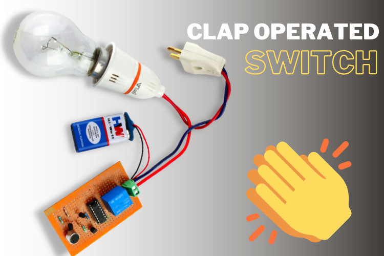
Final project looks like this.

Troubleshooting
Circuit not working?You must check all the connections according to the circuit diagram. A proper rating of components is a must usage here. Cross-check the soldering joints if you have missed anything to solder. Check for the bridges you might have made during soldering.
Load is getting ON instead of getting OFF?This means that you have connected your load to a normally closed (NC) terminal of the relay. Desolder the NC connection and solder it to the normally open (NO) pin of the relay.
Why we have grounded pin no.13 of IC?
Pin no. 13 is an Active low pin which means IC will work only when the pin is provided with low voltage.